What is 555 Timer IC
The 555 timer IC is a highly versatile and widely used integrated circuit (IC) in electronics. It was invented by Hans Camenzind in 1972 for Signetics (now part of ON Semiconductor). The IC can be used for a variety of timing and pulse generation applications.
The 555 Timer Can Operate in Three Main Modes:
Monostable mode – It acts as a one-shot pulse generator. When triggered, it produces a single output pulse for a specific duration.
Astable mode – Astable Mode Of 555 Timer acts as an oscillator, generating a continuous square wave (good for blinking LEDs, tone generation, etc.).
Bistable mode – It works like a flip-flop. It has two stable states and can toggle between them (used for switches and memory elements).
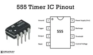
Pinout (8-pin DIP)
Pin | Name | Function |
1 | GND | Ground (0V) |
2 | Trigger | Starts the timing cycle when voltage < 1/3 Vcc |
3 | Output | The output signal (HIGH or LOW) |
4 | Reset | Resets the timer (active LOW) |
5 | Control | Voltage control (optional; usually with a capacitor to GND) |
6 | Threshold | Ends timing when voltage > 2/3 Vcc |
7 | Discharge | Discharges the timing capacitor |
8 | Vcc | Supply voltage (typically 5V to 15V) |
Common Applications
- LED flashers and blinkers
- Tone generators
- Timers and delay circuits
- Pulse-width modulation (PWM)
- Frequency generators
- Switch debouncing
- Simple logic clocks
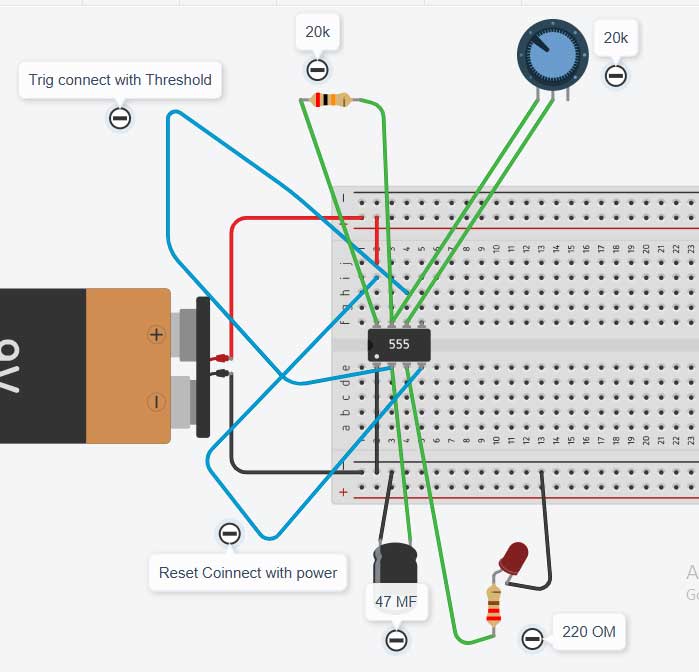
Example: 555 Timer in Astable Mode
- A common circuit setup makes the 555 produce a square wave:
- A capacitor and two resistors determine the frequency and duty cycle.
- Output toggles between HIGH and LOW continuously.
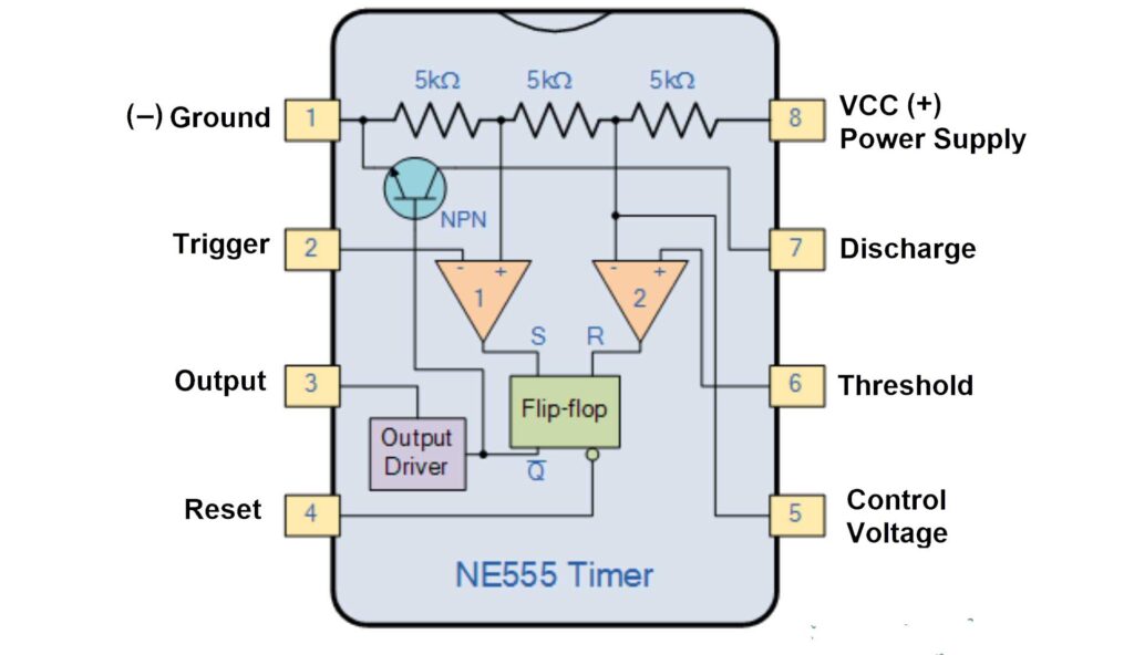
Key Components Inside the 555 Timer IC
Voltage Divider:
Three 5kΩ resistors in series divide the supply voltage into:
2/3 Vcc
1/3 Vcc
Two Comparators:
Comparator 1 compares the threshold voltage (pin 6) with 2/3 Vcc.
Comparator 2 compares the trigger voltage (pin 2) with 1/3 Vcc.
SR Flip-Flop (Set-Reset Latch):
Stores the output state.
Set by Comparator 2 and Reset by Comparator 1.
Discharge Transistor (NPN):
Connected to pin 7.
Discharges the timing capacitor to GND when ON.
Output Stage:
Push-pull output driver capable of sourcing or sinking current at pin 3.
Reset (pin 4):
Overrides all other inputs when pulled LOW; forces output LOW.
Working Principle
In Monostable Mode (One-shot pulse)
Initial state: Output is LOW.
When trigger pin goes below 1/3 Vcc, Comparator 2 sets the flip-flop → Output goes HIGH.
The capacitor begins charging through a resistor.
When the threshold pin reaches 2/3 Vcc, Comparator 1 resets the flip-flop → Output goes LOW.
The discharge transistor turns ON and discharges the capacitor.
Astable Mode Of 555 Timer (Oscillator)
No stable state.
Capacitor charges and discharges between 1/3 Vcc and 2/3 Vcc.
Comparators continuously toggle the flip-flop → square wave output is generated.
Frequency and duty cycle are set by external resistors and capacitor.
In Bistable Mode (Flip-flop)
Trigger and Reset pins are used to toggle the output state manually.
No timing capacitor is needed.
Summary
Feature | Description |
Operating Voltage | 4.5V – 15V |
Output Current | ~200 mA (sourcing/sinking) |
Typical Frequency Range | Up to 500 kHz |
Modes of Operation | Monostable, Astable, Bistable |
Internal Components | 2 Comparators, Flip-Flop, Discharge Transistor, Voltage Divider |
Best Use Of Arduino With Ultrasonic Sensor
Best Use Of Arduino With Relay